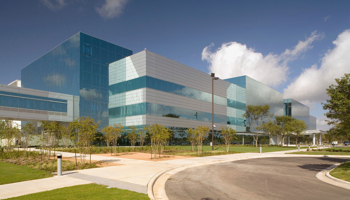
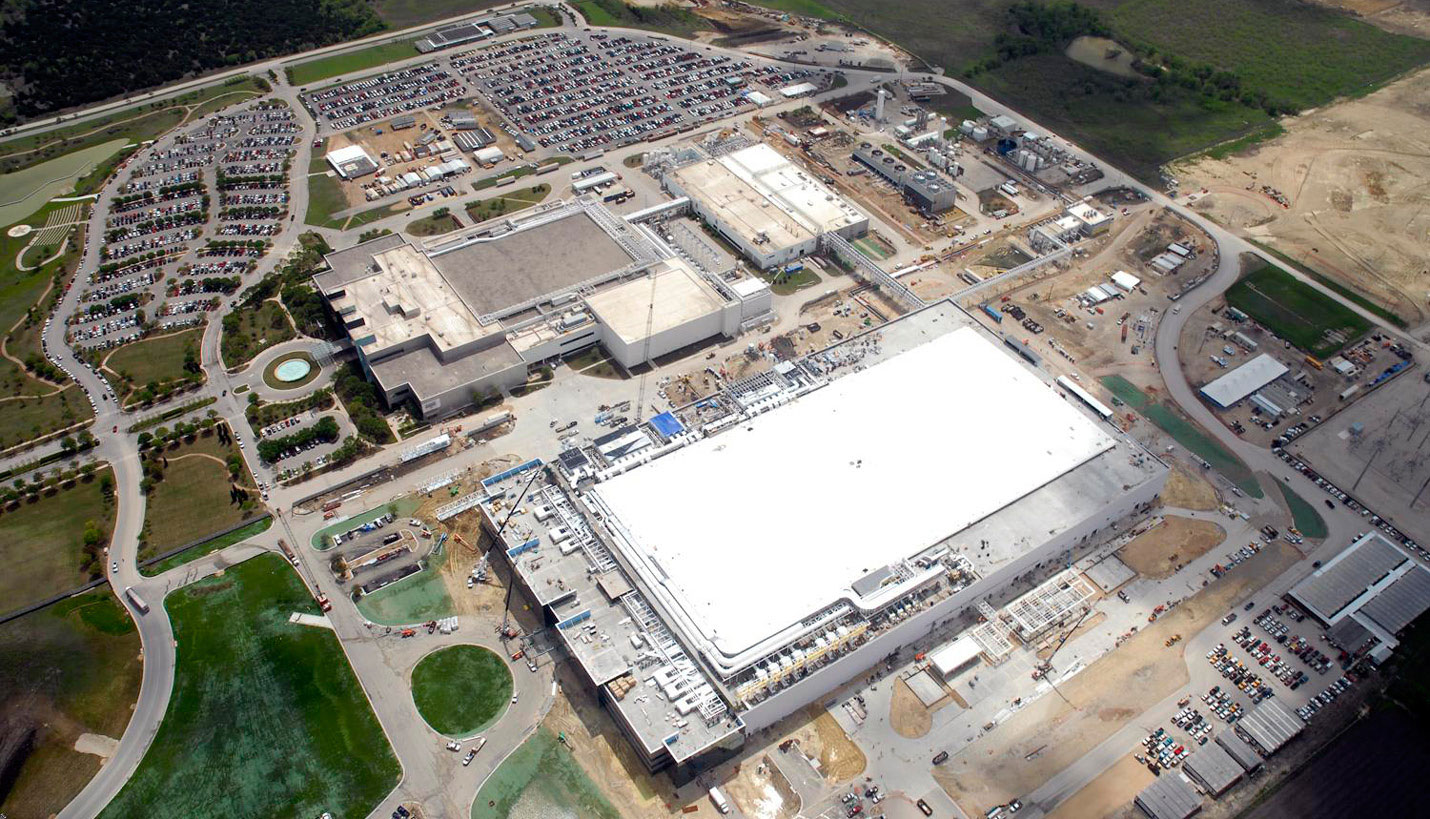
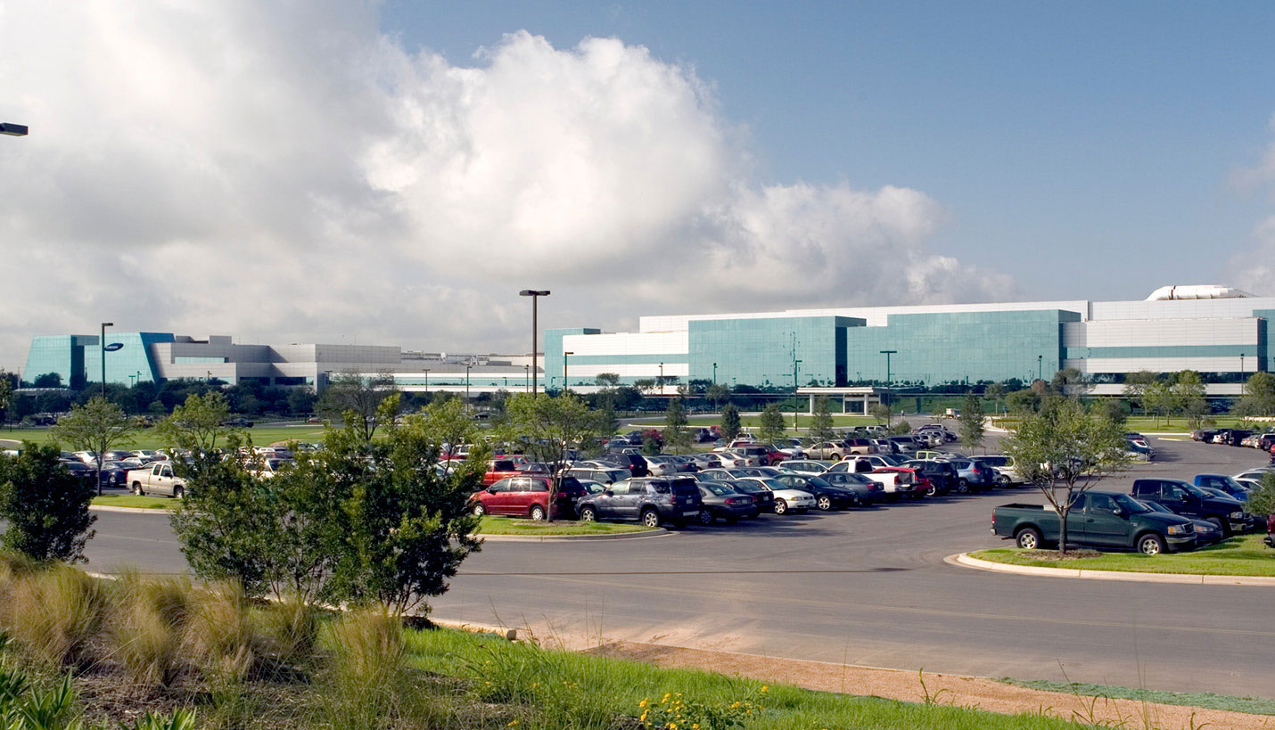
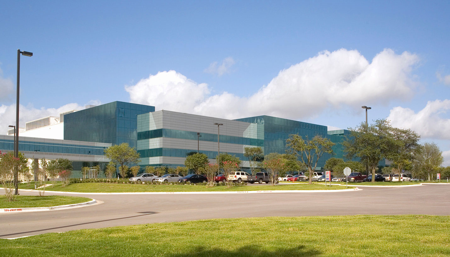
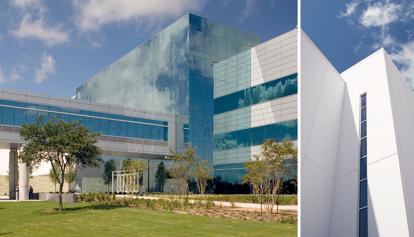
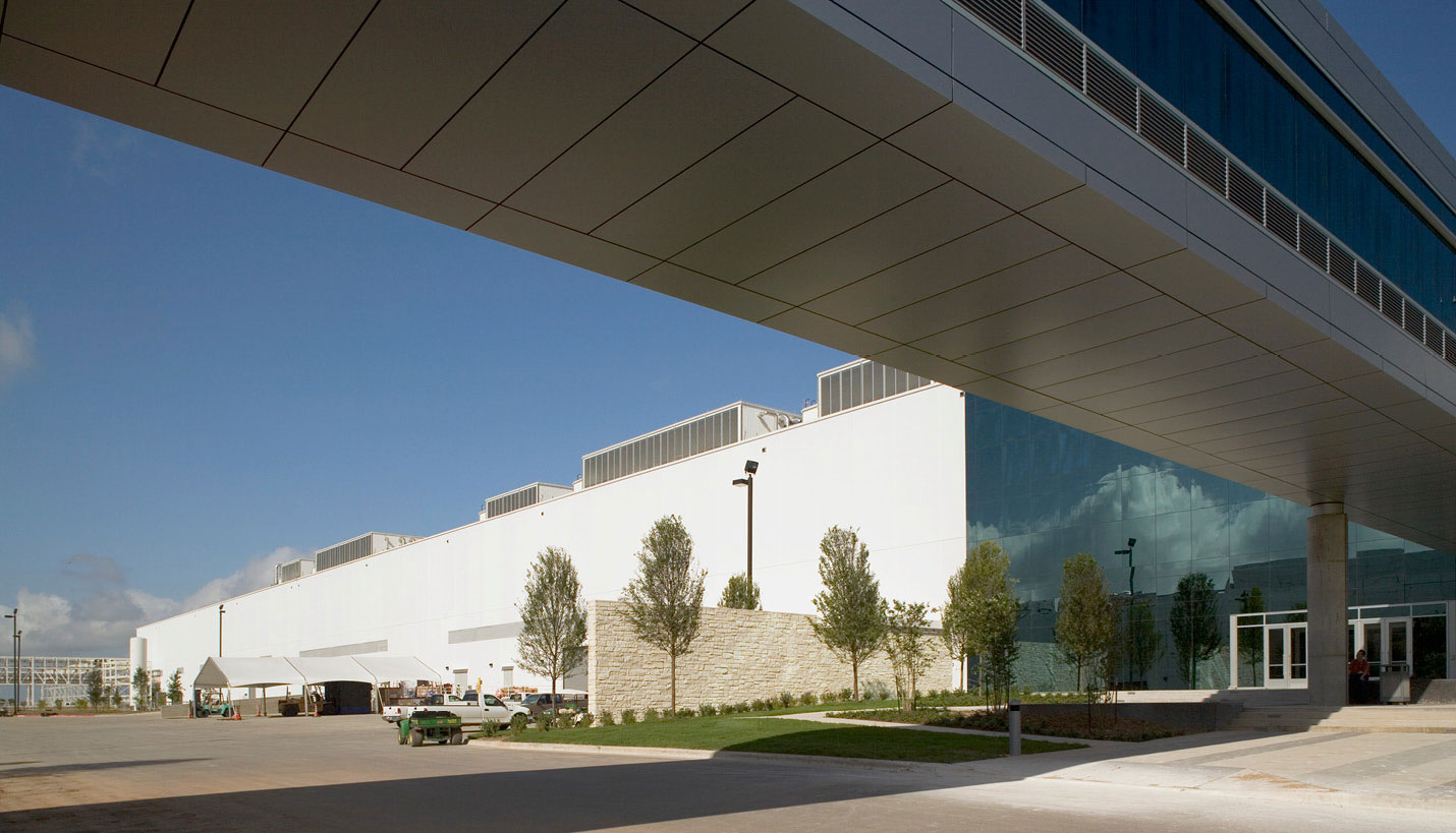
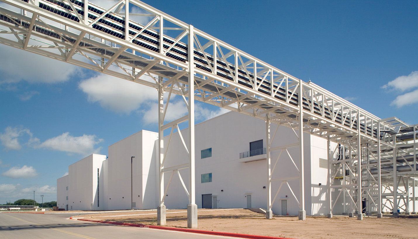
The Samsung Austin Semiconductor Fab A2, at the time of its construction, was the largest wafer fabrication facility in the United States. The 1.6 million-square-foot, 300MM plant includes 350,000 square feet of Class 100 cleanroom (including over 55 piping systems); 225,000 square feet of office support area; expansion to the existing central utility building and miscellaneous structures and support facilities.
Page architects and engineers converted 800 sheets of design drawings from Korea into 4,300 construction documents based on United States standards and English measurements and adapted them to the Austin site. Construction documents were issued in a “just-in-time” method of construction which enabled the project to be completed in a little over one year.